Semiconductors are materials which have a conductivity between conductors (generally metals) and non-conductors or insulators (such as most ceramics). Semiconductors can be pure elements, such as silicon or germanium, or compounds such as gallium arsenide or cadmium selenide.
A semiconductor device is an electronic component that relies on the electronic properties of a semiconductor material (primarily silicon, germanium, and gallium arsenide, as well as organic semiconductors) for its function. Semiconductor devices have replaced vacuum tubes in most applications.
Classification of Metals, Conductors and Semiconductors
On the basis of conductivity
On the basis of the relative values of electrical conductivity (σ ) or resistivity (ρ = 1/σ ), the solids are broadly classified as:
(i) Metals: They possess very low resistivity (or high conductivity).
ρ ~ 10–2 – 10–8 Ω m
σ ~ 102 – 108 S m–1
(ii) Semiconductors: They have resistivity or conductivity intermediate to metals and insulators.
ρ ~ 10–5 – 106 Ω m
σ ~ 105 – 10–6 S m–1
(iii)Insulators: They have high resistivity (or low conductivity).
ρ ~ 1011 – 1019 Ω m
σ ~ 10–11 – 10–19 S m–1
Elemental semiconductors: Si and Ge
Compound semiconductors: Examples are:
- Inorganic: CdS, GaAs, CdSe, InP, etc.
- Organic: anthracene, doped pthalocyanines, etc.
- Organic polymers: polypyrrole, polyaniline, polythiophene, etc.
Most of the currently available semiconductor devices are based on elemental semiconductors Si or Ge and compound inorganic semiconductors.
On the basis of energy bands
According to the Bohr atomic model, in an isolated atom the energy of any of its electrons is decided by the orbit in which it revolves. But when the atoms come together to form a solid they are close to each other. So the outer orbits of electrons from neighbouring atoms would come very close or could even overlap. This would make the nature of electron motion in a solid very different from that in an isolated atom.
In case of metallic conductors, conduction band overlaps on the electrons in the valence band.
In insulators, there is a large gap between both these bands. Hence, the electrons in the valence band remain bound and no free electrons are available in the conduction band.
Semiconductors have a small gap between both these bands. Some valence electrons gain energy from external sources and cross the gap between the valence and conduction bands. By this movement, they create a free electron in the conduction band and a vacant energy level in the valence band for other valence electrons to move. This creates the possibility of conduction.
Intrinsic Semiconductor
An intrinsic semiconductor is a semiconductor in which no other material is intentionally doped (similar to mixing). Example: Si, Ge.
An intrinsic (pure) semiconductor, also called an undoped semiconductor or i-type semiconductor, is a pure semiconductor without any significant dopant species present. The number of charge carriers is therefore determined by the properties of the material itself instead of the amount of impurities.
Extrinsic Semiconductor
The conductivity of an intrinsic semiconductor depends on its temperature, but at room temperature its conductivity is very low. As such, no important electronic devices can be developed using these semiconductors. Hence there is a necessity of improving their conductivity. This can be done by making use of impurities.
There are two types of dopants used in doping the tetravalent Si or Ge:
(i) Pentavalent (valency 5); like Arsenic (As), Antimony (Sb), Phosphorous (P), etc.
(ii) Trivalent (valency 3); like Indium (In), Boron (B), Aluminium (Al), etc.
(i) n-type semiconductor
An n-type semiconductor is an intrinsic semiconductor doped with phosphorus (P), arsenic (As), or antimony (Sb) as an impurity. Silicon of Group IV has four valence electrons and phosphorus of Group V has five valence electrons. If a small amount of phosphorus is added to a pure silicon crystal, one of the valence electrons of phosphorus becomes free to move around (free electron*) as a surplus electron. When this free electron is attracted to the “+” electrode and moves, current flows.
(ii) p-type semiconductor
A p-type semiconductor is a type of semiconductor. When the trivalent impurity is added to an intrinsic or pure semiconductor (silicon or germanium), it is said to be a p-type semiconductor. Trivalent impurities such as boron (B), gallium (Ga), indium (In), aluminium (Al) etc. are called acceptor impurity.
p-n Junction
A p-n junction is the basic building block of many semiconductor devices like diodes, transistor, etc. A clear understanding of the junction behaviour is important to analyse the working of other semiconductor devices.
p-n junction formation
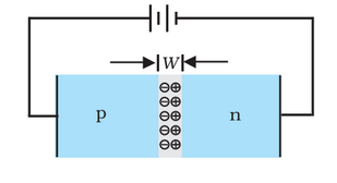
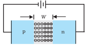
P-n junctions are formed by joining n-type and p-type semiconductor materials, as shown below. Since the n-type region has a high electron concentration and the p-type a high hole concentration, electrons diffuse from the n-type side to the p-type side.
Semiconductor Diode
A semiconductor diode is basically a p-n junction with metallic contacts provided at the ends for the application of an external voltage. It is a two terminal device.
p-n junction diode under forward
A P-N junction diode is said to be forward biased when the positive terminal of a cell or battery is connected to the p-side of the junction and the negative terminal to the n side. When diode is forward-biased the depletion region narrows and consequently, the potential barrier is lowered.
When an external voltage V is applied across a semiconductor diode such that p-side is connected to the positive terminal of the battery and n-side to the negative terminal, it is said to be forward biased.
p-n junction diode under reverse bias
The process by which, a p-n junction diode blocks the electric current in the presence of applied voltage is called reverse biased p-n junction diode. These positive ions at p-n junction (n-side) oppose the flow of positive charge carriers (holes) from p-side.
When an external voltage (V) is applied across the diode such that n-side is positive and p-side is negative, it is said to be reverse biased. The applied voltage mostly drops across the depletion region.
Application of Junction Diode as a Rectifier
The main application of p-n junction diode is in rectification circuits. These circuits are used to describe the conversion of a.c signals to d.c in power supplies. Diode rectifier gives an alternating voltage which pulsates in accordance with time. The filter smoothes the pulsation in the voltage and to produce d.c voltage, a regulator is used which removes the ripples. There are two primary methods of diode rectification:
- Half Wave Rectifier
- Full Wave Rectifier
Special Purpose p-n Junction Diodes
This is a special p-n junction diode operated in reverse bias and designed with a transparent window to allow light to fall on it. When photons with energy (hv) greater than the energy gap of the semiconductor fall on it, electron-hole pairs are generated.
Zener diode
A Zener diode is a special type of diode designed to reliably allow current to flow "backwards" when a certain set reverse voltage, known as the Zener voltage, is reached.
Zener diodes are used for voltage regulation, as reference elements, surge suppressors, and in switching applications and clipper circuits. The load voltage equals breakdown voltage VZ of the diode. The series resistor limits the current through the diode and drops the excess voltage when the diode is conducting.
Zener diode as a voltage regulator: A zener diode is always operated in its reverse biased condition. As such a simple voltage regulator circuit can be designed using a zener diode to maintain a constant DC output voltage across the load in spite of variations in the input voltage or changes in the load current.
Optoelectronic junction devices
Optoelectronic devices are electrical-to-optical or optical-to-electrical transducers, or instruments that use such devices in their operation. Optoelectronics is based on the quantum mechanical effects of light on electronic materials, especially semiconductors, sometimes in the presence of electric fields.
Photodiode: A photodiode is a semiconductor p-n junction device that converts light into an electrical current. The current is generated when photons are absorbed in the photodiode. Photodiodes may contain optical filters, built-in lenses, and may have large or small surface areas.
Light emitting diode: A light-emitting diode (LED) is a semiconductor light source that emits light when current flows through it. Electrons in the semiconductor recombine with electron holes, releasing energy in the form of photons. The first visible-light LEDs were of low intensity and limited to red. LEDs have the following advantages over conventional incandescent low power lamps:
- Low operational voltage and less power.
- Fast action and no warm-up time required.
- The bandwidth of emitted light is 100 Å to 500 Å or in other words it
- is nearly (but not exactly) monochromatic.
- Long life and ruggedness.
- Fast on-off switching capability.
Solar cell: A solar cell is basically a p-n junction which generates emf when solar radiation falls on the p-n junction. It works on the same principle (photovoltaic effect) as the photodiode, except that no external bias is applied and the junction area is kept much larger for solar radiation to be incident because we are interested in more power.
Junction Transistor
A Bipolar Junction Transistor is a semiconductor device consisting of two P-N Junctions connecting three terminals called the Base, Emitter and Collector terminals. The arrangement of the three terminals affects the current and the amplification of the transistor.
The credit of inventing the transistor in the year 1947 goes to J. Bardeen and W.H. Brattain of Bell Telephone Laboratories, U.S.A. That transistor was a point-contact transistor. The first junction transistor consisting of two back-to-back p-n junctions was invented by William Schockley in 1951.
Transistor: structure and action
A transistor has three doped regions forming two p-n junctions between them. Obviously, there are two types of transistors
(i) n-p-n transistor: Here two segments of n-type semiconductor (emitter and collector) are separated by a segment of p-type semiconductor (base).
(ii) p-n-p transistor: Here two segments of p-type semiconductor (termed as emitter and collector) are separated by a segment of n-type semiconductor (termed as base).
A brief description of the three segments of a transistor is given below:
- Emitter: This is the segment on one side of the transistor shown in. It is of moderate size and heavily doped. It supplies a large number of majority carriers for the current flow through the transistor.
- Base: This is the central segment. It is very thin and lightly doped.
- Collector: This segment collects a major portion of the majority carriers supplied by the emitter. The collector side is moderately doped and larger in size as compared to the emitter.
Basic transistor circuit configurations and transistor characteristics
In a transistor, only three terminals are available, viz., Emitter (E), Base (B) and Collector (C). Therefore, in a circuit the input/output connections have to be such that one of these (E, B or C) is common to both the input and the output. Accordingly, the transistor can be connected in either of the following three configurations: Common Emitter (CE), Common Base (CB), Common Collector (CC).
Transistor as a device
The transistor can be used as a device application depending on the configuration used (namely CB, CC and CE), the biasing of the E-B and B-C junction and the operation region namely cut off, active region and saturation. As mentioned earlier we have confined only to the CE configuration and will be concentrating on the biasing and the operation region to understand the working of a device.
(i) Transistor as a switch: With a zero signal applied to the Base of the transistor it turns “OFF” acting like an open switch and zero collector current flows. With a positive signal applied to the Base of the transistor it turns “ON” acting like a closed switch and maximum circuit current flows through the device.
(ii) Transistor as an amplifier: A transistor acts as an amplifier by raising the strength of a weak signal. The DC bias voltage applied to the emitter base junction, makes it remain in forward biased condition. Thus a small input voltage results in a large output voltage, which shows that the transistor works as an amplifier.
Transistor as an Amplifier (CE-Configuration)
The common emitter transistor amplifier is the only configuration that gives an inversion, 180°, between the input and output signals. The reason for this can be seen from the fact that as the input voltage rises, so the current increases through the base circuit.
Feedback amplifier and transistor oscillator
In a feedback amplifier and transistor oscillator, the oscillator generates an amplified output signal without any intake of input signals. The working of an oscillator is a repetitive process with the amplified input and output resulting in feedback with persistent operations.
Digital Electronics and Logic Gates
Digital electronics is a field of electronics involving the study of digital signals and the engineering of devices that use or produce them. This is in contrast to analog electronics and analog signals.
Logic gates
Logic gates are the basic building blocks of any digital system. It is an electronic circuit having one or more than one input and only one output. The relationship between the input and the output is based on a certain logic. Based on this, logic gates are named as AND gate, OR gate, NOT gate etc.
(i) NOT gate: This is the most basic gate, with one input and one output. It produces a ‘1’ output if the input is ‘0’ and vice-versa. That is, it produces an inverted version of the input at its output. This is why it is also known as an inverter.
(ii) OR Gate: An OR gate has two or more inputs with one output. The output Y is 1 when either input A or input B or both are 1s, that is, if any of the input is high, the output is high.
(iii) AND Gate: An AND gate has two or more inputs and one output. The output Y of AND gate is 1 only when input A and input B are both 1.
(iv) NAND Gate: This is an AND gate followed by a NOT gate. If inputs A and B are both ‘1’, the output Y is not ‘1’. The gate gets its name from this NOT AND behaviour.
(v) NOR Gate: It has two or more inputs and one output. A NOT- operation applied after OR gate gives a NOT-OR gate (or simply NOR gate). Its output Y is ‘1’ only when both inputs A and B are ‘0’, i.e., neither one input nor the other is ‘1’.
Integrated Circuits
Integrated circuit (IC), also called microelectronic circuit, microchip, or chip, an assembly of electronic components, fabricated as a single unit, in which miniaturized active devices (e.g., transistors and diodes) and passive devices (e.g., capacitors and resistors) and their interconnections are built up on a thin substrate of semiconductor material (typically silicon). The resulting circuit is thus a small monolithic “chip,” which may be as small as a few square centimetres or only a few square millimetres. The individual circuit components are generally microscopic in size.