Questions
1
The manifestation of band structure in solids is due to
Answer:Pauli’s exclusion principle
3
If the energy of a photon of sodium light (A = 589 nm) equals the band gap of semiconductor, the minimum energy required to create hole electron pair
Answer:2.1 eV
4
In a half wave rectifier circuit operating from 50 Hz mains frequency, the fundamental frequency in the ripple would be
Answer:50 H
5
What happens during regulation action of a Zener diode?
Answer:Both (a) and (b)
6
In good conducrors of electricity the type of bonding that exist is
Answer:metallic
7
Carbon, silicon and germanium have four valence electrons each. These are characterised by valence and conduction bands separated by energy band gap respectively equal to (E^)c, (Eg)Si and (Eg)Ge. Which of the following statements is true?
Answer:(Eg)C < (Eg)Si < (Eg)Ge
8
A zener diode is specified as having a breakdown voltage of 9.1 V, with a maximum power dissipation of 364 mW. What is the maximum current the diode can handle?
Answer:40 mA
9
If in a n-type semiconductor when all donor states are filled, then the net charge density in the donor states becomes
Answer:> 1
10
The breakdown in a reverse biased p-n junction diode is more likely to occur due to
Answer:large velocity of the minority charge carriers if the doping concentration is large
11
Region without free electrons and holes in a p-n junction is
Answer:depletion region
12
The probability of electrons to be found in the conduction band of an intrinsic semiconductor of finite temperature
Answer:decreases exponentially with increasing band gap
13
In the circuit shown if current for the diode is 20 μA, the potential difference across the diode is
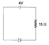
Answer:4 V
14
Potential barrier developed in a junction diode opposes the flow of
Answer:majority carriers only
15
In an n-type silicon, which of the following statements is true.
Answer:Holes are minority carriers and pentavalent atoms are the dopants.
16
Which of the following statements is incorrect for the depletion region of a diode?
Answer:There the mobile charges exist.
17
If a small amount of antimony is added to germanium crystal
Answer:there will be more free electrons than holes in the semiconductor,
18
The dominant mechanism for motion of charge carriers in forward and reverse biased silicon p-n junction are
Answer:diffusion in forward bias, drift in reverse bias
19
In an unbiased p-n junction, holes diffuse from the p-region to n-region because
Answer:hole concentration in p-region is more as compared to u-region.
20
To obtain electrons as majority charge carriers in a semiconductors the impurity mixed is:
Answer:divalent
Chapters
- Electric Charges & Fields
- Electrostatic potential and capacitance
- Electricity
- Moving charges and magnetism
- Magnetism and matter
- Electromagnetic induction
- Alternating current
- Electromagnetic waves
- Ray optics and optical instruments
- Wave optics
- Dual nature of radiation and matter
- Atoms
- Nuclei
- Semiconductor electronics
- Communication systems